In the design planning context, floorplanning is the process of sizing, shaping, and placing hierarchical cells and functional blocks in a manner that makes later physical design steps more effective. Overall, floorplanning is an important stage in physical design because it directly impacts the performance, power consumption, and area utilization of the final chip. A well-executed floorplan can significantly reduce design iterations and shorten time-to-market, making it an essential step in the chip design process.
Main aim of the floorplan is: -
- Minimize the area.
- Minimize the total wire length.
- Improve routability.
- Minimize delay.
- Minimize cost
Floorplanning in hierarchical flows provides a basis for estimating the timing of the top level. A timing budget allocates the clock cycle time to each block according to the top-level timing estimation. An effective floorplan helps ensure timing closure in many ways, such as placing blocks to make critical paths short, preventing routing congestion that would lead to longer paths, and eliminating the need for over-the-top routing for noise-sensitive blocks. The challenge is to create a floorplan with good area efficiency while leaving sufficient area for standard cell placement and signal and clock routing.
In the floorplan, the size and shape of the chip or block are defined. Macro and IO cell placement is getting placed in such a way that effective routing space is available between the channel region and between the macro and IO regions. For standard cell placement, we keep the contiguous core area for standard cell placement and optimization strategy from the target cell library.

Fig1: Standard Cell Placement with Design Hierarchy GUI Image
II. FLOORPLAN STEPS, GUIDELINES, AND TECHNIQUES
The inputs to floorplan are gate-level netlist, libraries (logical and physical/reference), timing
During the floorplan the following steps are to be done.
- Initialization of a floorplan of appropriate dimension.
- Macro Placement. Placement of I/O pins.
- Macro placement considers the communication between them through fly lines.
- Creation of power strap
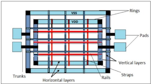
Fig2: Power Planning Illustration [Image Source: Adam Teman] - Applying appropriate placement blockages near the macros, near the I/O pins, densely packed cell areas, etc.
- Placement of tap cells and boundary cells and endcap cells.
B] Floorplan Guidelines
- The placement of macros is based on the fly-lines (it shows the connectivity b/w macro to macro and macro to standard cell), so we can minimize the interconnect length between IO pins and other cells.
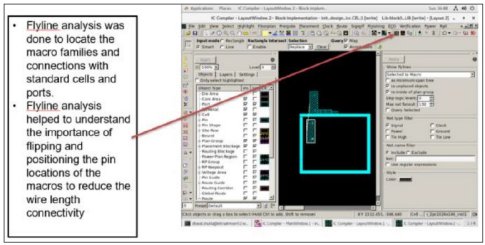
Fig3: Macro placement using flyline analysis. - During the initial floorplan placement, we shall perform fly line analysis followed by fanin-fanout techniques during the next floorplan iterations. This will help us to converge design with less iteration.
- Place the macros around the boundary of the core, leaving some space between the macro to the core edge so that during optimization this space will be used for buffer/inverter insertion and keeping large areas at the centre of the core area for placement of standard cells during the placement stage.
- Macros that are communicating with pins/ports of the core place near to core boundary.
- Place the macros of the same hierarchy together.
- Keep a sufficient channel between macros.
- Avoid notches while placing macros, if anywhere notches are present then use hard blockages in that area.
- Avoid notches while placing macros, if anywhere notches are present then use hard blockages in that area.
- Avoid crisscross connection of macro placement.
- Create a keep-out margin around the four sides of macros, so no standard cells will not get placed near macro pins. This technique avoids congestion.
- Keep placement blockages at the corner of macros.
- For the pin side of macros keep a larger separation and for the non-pin side, we can abut/adjoin the macros with their halo, so that area will be saved and the halo of two macros can be abutted so that no standard cells are placed in between macros.
- Between two macros at least one pair of power straps (power and ground) should be present for a non-abutted floorplan.
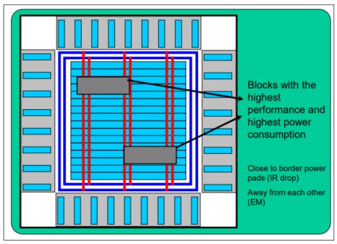
Fig 4: Power Plan Strategy [Image Source: Adam Teman]
- Multiple iterations happen to achieve an optimum floorplan. The chip designer takes care of the design parameters such as power, area, and performance during floorplan stage.
III. SANITY CHECKS BEFORE FLOORPLAN
By performing sanity checks, we ensure that the input received from the library and synthesis teams is correct. Nonperformance of sanity checks leads to creating problems in the later stages of design. There are three sanity checks, i.e., design/netlist checks, SDC Checks, and library checks.
A] Design/Netlist Checks:
- Check if the current design is consistent or not. Checks like
- floating pins, muti-driven nets, undriven input ports, unloaded outputs, unconstrained pin, pin mismatch count between an instance and its reference, tristate buses with non-tristate drivers, and wire loops across hierarchies.
- check_design command in ICC II checks for multi-driven nets, floating nets/pins, empty modules, pin mismatches, cells, or instances without IO pins/ports, etc.
B] SDC or Timing Checks:
- If any unconstrained path exists in the design, then the PnR tool will not optimize that path, so these checks are used to report unconstrained paths.
- Using check_timing in ICC II, we can perform checks on whether the clock is reaching all the clock pins of the flip-flop, check if multiple clocks are driving the same registers, check if unconstrained endpoints, Port missing input/output delay, check port missing slew/load constraints.
C] Library Checks:
- It validates the library. i.e., checks the consistency between logical and physical libraries.
- It checks the qualities of both libraries.
- check_library command is used for library checks in ICC II. This command shows the name of the library, library types and their version, units of time, capacitance, leakage power, and current. It shows the number of cells missing, and the number of metal or pins missing in the physical and logical library.
IV. INITIAL FLOORPLAN AND DIE SIZE ESTIMATION
Once the netlist is read into the database, we perform an initial floorplan to determine the dimensions of the chip as well as critical macro locations. The main goals of the initial floorplan are to arrive at the optimum shape, and size, to achieve the smallest die size to reduce the cost of the total chip, and to be aware of signal integrity issues. The cost for the total chip depends mainly on the used space on silicon. In the future, it is not enough to pay more attention to die size alone. The signal integrity issues like crosstalk, electromigration, hot electron, and wire self-heat become more important issues in deep submicron (DSM) designs, and this influences the die size seriously.
Die size estimation.
- Technology inputs: gate density per sq. mm =D; the number of horizontal layers= H; the number of vertical layers=V
- Design inputs: gate count (excluding memories, macro & sub chip) = G; IO area, in sq. mm=I; Memory + Macro + Sub chip area, in sq. mm =M; target utilization, in percentage=U%; Additional gate count for CTS, timing closure etc., in percentage=T%; Additional gate count for ECO, in percentage=E%
Die area calculation.
- Die Area in sq.mm = {[(Gate count + Additional gate count for CTS & ECO) / Gate density] + IO area + Mem, Macro area} / Target utilization Die Area
= {[(G + T + E) / D] + I + M} / U
Limitations for setting up the die size.
In core-limited design, core is densely packaged and in IO or pad-limited design IOs/pads are densely packed which limits the size of the chip.
a) pad-limited: In this design, there are so many pads that each pad is directly placed adjacent to the next pad. Although there is a small core area it is not possible to get a smaller die size.
- The inputs and outputs from the chip are called Pads; they are located at the outline of the die boundary.
- The position of these cells may change when the floorplan is modified.
- Types of pads: 1. Input pads & Output pads for the required input & output signals; 2. Bi-directional pads for bi-directional signals like buses; 3. Power and Ground pads to provide the required supply voltage.
- Pads establish contact between the chip and the pins of the package.
- They protect the chip against electrostatic discharge.
- They work as amplifiers to boost the input and the output signals.
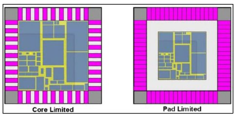
Fig 5: Image Source: Adam Teman
b) Core limited: The Standard cells in the core need so much space that a smaller die size is not possible. Here the pads are not placed directly next to each other.
c) Block limited: The Design contains many macro blocks. It is not possible to place these macro blocks closer together to get a smaller die size.
d) Package limited: If the Package for the design is chosen before the die size is set up the package limits the maximum die size because each package has a maximum space for the die.
V. TYPES OF FLOORPLANS, CONTROL PARAMETERS, AND CORE UTILIZATION
A] Types of floorplans in full-chip design
- Abutted Floorplan: Channel-less placement of blocks.
- Non-Abutted Floorplan: Channel-based placement of blocks.
Channel Width = (No. of Pins * Pitch)/ No. of Layers either H/V. - Mixed/Partially Abutted: Partially abutment of blocks with channels in certain areas.
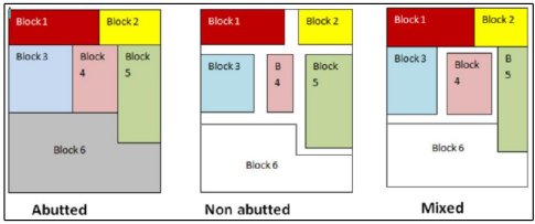
Fig 6: Different Types of Floorplans [ Image Source: Adam Teman]
B] Floorplan control parameters
- Aspect ratio, width, and height calculation
- o The aspect ratio is defined as the ratio of height to width.
- A. R= height/width
= Number of horizontal resources/ Number of vertical resources = H/V - A. R= H/W → H = W*A. R ----- (1)
- Die Area= W*H = W*W*A. R [Expressing H in terms of W from (1)]
- W^2 = Die Area/A. R → W = sqrt (Die Area/AR)
- A. R= height/width
- o The aspect ratio is defined as the ratio of height to width.
Odd aspect ratios result in too much congestion and timing issues. It can be greater than 1, less than 1, or equal to 1 (which is preferred) i.e., squarish.
Note:
- Most of the algorithms work better when the floorplan is squarish. If there are notches in the floorplan, the router needs to spend more effort to clean up the DRCs.
- Special care must be taken when there are notches to ensure that placement/routing density is not high on the edges etc.
- Cell placement can be proper in squarish floorplans and hence timing can be met easily.
- If the aspect ratio is close to 1 then there is more availability of routing resources in both horizontal & vertical directions.
- The aspect ratio should consider the number of routing resources available.
- If there are more horizontal layers, then the rectangle should be long, and the width should be small, and vice versa if there are more vertical layers in the design.
C] Core Utilization
- Utilization will define the area occupied by the standard cells, macros, and other cells. If core utilization is 0.6 (60%) that means 60% of the core area is used for placing the standard cells, macros, and other cells, and the remaining 40% is used for routing purposes.
- Core: The Core is defined as the inner block, which contains the standard cells and macros. There is another outer block that covers the inner block. The I/O pins are placed on the outer block.
- Concept of row: The standard cells in the design are placed in standard cell rows. All the standard cell rows have equal height and spacing between them. The width of the standard cell rows can vary. The standard cells in the rows get the power and ground connection from VDD and VSS rails, which are placed on either side of the cell rows. Sometimes, technology allows the rows to be flipped or abutted, so that they can share the power and ground rails.
Standard cell row utilization
- It is defined as the ratio of the area of the standard Cells to the area of the chip minus the area of the macros and the area of blockages.
- Area (Standard Cells) / {Area (Chip) – Area (Macro) – Area (Region Blockages)}
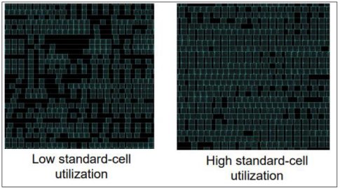
Fig7: Standard Cell Row Utilization [ Image Source: Adam Teman]
VI. I/O PLACEMENT, TYPES OF BLOCKAGES, AND SPECIAL CELLS
A] IO Placement
- The I/O cells are the ones that interact in between the blocks outside of the chip and with the internal blocks of the chip.
- In the floorplan, these I/O cells are placed between the inner ring (core) and the outer ring (chip boundary).
- These I/O cells are responsible for providing voltage to the cells in the core.
There are two types of I/O:
- Chip IO: The chip contains I/O pins. The chip consists of the core, which contains all the standard cells, and blocks. The chip I/O placement consists of the placement of I/O pins and the I/O pads. The placement of these I/O pads depends on the type of packaging.
- Block IO: The core contains several blocks. Each block contains the Block I/O pins, which communicate with other blocks and cells in the chip. Pin placement is an important step in the floor plan, which can be optimized based on pin placement requirements. The pin placement can be done based on timing, congestion, and utilization of the chip. Pin placement in macros utilizes M3 layers most of the time, so the macro needs to be placed logically. The logical way is to put the macros near the boundary. If there is no connectivity between the macro pins and the boundary, then move it to another location.
B] Placement Blockages
- When placing large macros, we must consider impacts on routing, timing, and power. Usually, push them to the sides of the floorplan. Placement algorithms generally perform better with a single large rectangular placement area. For wire-bond place power-hungry macros away from the chip center. After placing hard macros, mark them as fixed.
- Placement blockage halos are areas where the tools should not place any cells. Blockages are the specific location where the placing of cells is blocked. If the macros moved from one place to another place, blockages would not move. Blockages are of three types.ie., soft, hard, and partial.
- Soft blockages: Only a buffer can be placed. Prevent the placement of standard cell and hard macro within the specified area during coarse placement but allows placement of buffer/inverter during optimization, legalization, and clock tree synthesis.
- Hard blockages: No standard cells, macros, and buffer/inverter can be placed within the specified area during coarse placement, optimization, and legalization. Used to avoid routing congestion at macro corners. It controls the power rail generation at the macros.
- Partial blockages: Partial blockages limit the cell density in the specified area. By default, the blockage factor is 100% so no cell can be placed in that region. We can also modify the percentage by setting the blockage percentage factor as well.
- Halo/padding/keepout margin: An area outside a macro that should be kept clear of standard cells. This is the region around the fixed macros so that no other macros and the standard cell can be placed near to macro boundary. The width of the keepout margin on each side of the fixed cell can be the same or different depending on how you define keepout margin.
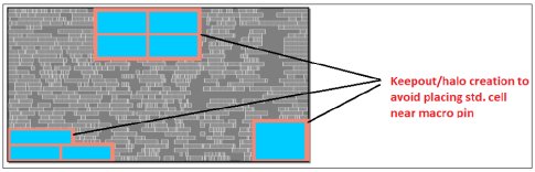
Fig 8: Setting macro keepout margin for avoiding congestion during std. cell placement. [Image Source: Adam Teman]
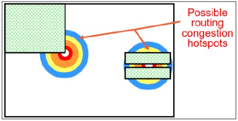
Fig 9: Congestion Hotspot [Image Source: Adam Teman]
C] Standard Cells
- Standard cells are nothing but base cells (Gates, Flops). It is a group of transistors and its interconnect structures that provide a Boolean logic function (e.g., AND, OR, XOR, XNOR, Inverter) or a storage function (Flip-flop or Latch). Standard cell methodology has helped the designer scale ASICs from comparatively simple single-function ICs, to complex multi-million gate SoCs.
- The cell-based methodology makes the designer focus on the implementation/physical aspects. The cell’s Boolean logic function is called its logical view. Functional behavior is captured in the form of the truth table or Boolean algebra equation (for combinational logic), or a state transition table (for sequential logic). AOIs/OAIs provide a way at the gate level to use fewer transistors than separate ANDs and NORs.
- Types of standard cells: Buffers/Inverters, Combinational (AND, OR, NAND, NOR, AOI, OAI, OA, AO, MUX). Arithmetic (XOR, Full-Adder, Half Adder), Sequential (latches, clock gates, D-FF with any optional combination of scan input, set, and reset), Miscellaneous (ICG Cells, Well Taps, Tie Cells, End Caps, Decaps, Filler Cells, Spare Cells, Delay Cells, Antenna Diode, ESD Diodes).
VII. QUALIFYING FLOORPLAN
- All macros should be placed and fixed.
- All IO pins must be placed and fixed.
- Block should have a uniform standard cell area.
- Avoid notches.
- Legality checks must pass.
- There should not be any overlaps between memories and blockages.
- Try to place memories across boundary areas unless it is not a design requirement to place them in the centre of the design.
- Blockages must be applied properly around the memories to avoid unnecessary congestion.
- There must be at least one VDD and VSS power strap between memories to avoid IR and to improve signal strength at the macro pin by inserting buffers.
- Try to maintain free space in front of ports to have easy access for standard cell talking.
- Pre-placement timing can be checked like IO timing, macro to macro timing, and macro to standard cell timing with margin after power plan.
- IR drop must be considered during synthesizing power networks for establishing connections of VDD/VSS rails and standard cells and macros VDD/VSS pin.
- There shall not be any floating pins and floating wires in the layout once the power plan is done.
The quality of the chip is defined by the quality of floorplan. A well-optimized floorplan results in more efficient utilization of the core area thereby aiding the placement of standard cells without causing an issue related to congestion, timing, IR drops, and signal integrity, etc. The bad floorplan affects the area, power, and reliability of chip functioning and requires more back annotation efforts and ECO activity for design closure, which increases overall IC cost also. Bad floorplan leads to worst timing and congestion issues, noise, IR, and EM issues.

Comments
Post a Comment