MODERN TECHNIQUES
Modern IC designs are heavily influenced by the need to minimize power consumption, particularly in the consumer electronics market. The devices' warmth, battery life, and the time it takes to switch on and off the functions of handheld devices are currently being reformed. Therefore, it becomes crucial to implement best practices in chip design to help reduce power consumption in SoCs (System on Chip). The power management of SoCs and RTL designs has a significant impact on the silicon's performance. Power-aware designs are used by industry to achieve power statistics. This blog focuses on multi-voltage design terms that can be used to assess the power performance of silicon in HDL coding. These facilitate the understanding of design parameters while implementing power-conscious designs.
Multi Voltage Power Domain
Power supply and dynamic power, which includes switching and short-circuit power, are directly related. Consequently, power performance is naturally improved by lowering power. The gate delay increases as a result of the lower threshold voltage. Perhaps the first design implementation utilized to achieve power performance goals is lowering the voltage of SoC blocks. The system displays various voltage levels in Figure 1.
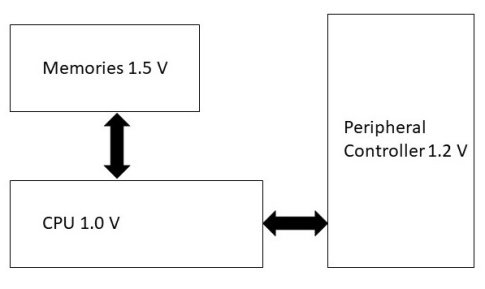
Figure 1
Lowering the voltage, lowers the current flowing and increases the delay in the gates, and by that means, the designs may not be able to run at desired clock frequencies. Lowering the voltage may cost the performance statistics but the performance can still be met as seen in Figure 1.
Figure 1
Lowering the voltage, lowers the current flowing and increases the delay in the gates, and by that means, the designs may not be able to run at desired clock frequencies. Lowering the voltage may cost the performance statistics but the performance can still be met as seen in Figure 1.
Figure 1 can also be referred to as a multi-VDD design. The logic is partitioned into different domains called power domains. The structural model or a gate-level netlist derived from behavioural Verilog uses a different voltage line for each domain. The individual domains can be run as per performance objectives. Figure 2 shows an elaboration of the same.
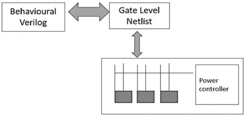
Figure 2
The power architect uses this technology to generate files that explain an electric design's power and power control intent. The annotation covers memory retention strategies, power switches, level shifters, and supply sets. Definable descriptions of the prospective power applied to the electronic system include power states, transitions, a group of sim states, the type and function features of nets to help refine the power intent gradually, and the -update parameter.
Requirements to create a multi-voltage design
Level shifters
As shown in figure 3. level shifters will shift the level of voltages to ensure different modules operating at different voltages will operate correctly when LS (Level shifter) circuits are attached. The circuits are implemented in HDL, and they can also be made to implement the drive strength. The figure shows a low to high voltage level shifter (A) and a high to low voltage level shifter (B). Vi and Vo are the sources and destinations of different voltage levels in different modules.
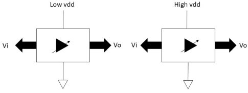
Figure 3
Power gating
The method in figure 4 is referred to as Disconnecting the power of the gates which are not in use. The figure shows an implementation of such a situation. Power gating is used to reduce leakage power. This step is performed at an architecture level while computing the performance factors of the low power module, or module at a sleep state while other priority modules are ON, or module where power is to be disconnected by software, or while shutting down the power.
Level shifters
As shown in figure 3. level shifters will shift the level of voltages to ensure different modules operating at different voltages will operate correctly when LS (Level shifter) circuits are attached. The circuits are implemented in HDL, and they can also be made to implement the drive strength. The figure shows a low to high voltage level shifter (A) and a high to low voltage level shifter (B). Vi and Vo are the sources and destinations of different voltage levels in different modules.
Figure 3
Power gating
The method in figure 4 is referred to as Disconnecting the power of the gates which are not in use. The figure shows an implementation of such a situation. Power gating is used to reduce leakage power. This step is performed at an architecture level while computing the performance factors of the low power module, or module at a sleep state while other priority modules are ON, or module where power is to be disconnected by software, or while shutting down the power.
Power gating is significantly used while modern-day traditional terms like SLEEP/WAKE events of the device. The wakeup and sleep sequence follow certain architectural decisions to enable or disable a sequence of operations that controls the power logic of the chip.
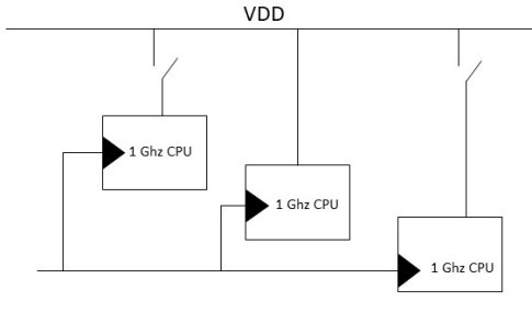
Figure 4
Special care must be taken while implementing power gating as output signals from a power gated block pose special challenges. This considers isolation and retention strategies at the micro-Architecture level while performing the wake-up or sleep sequence. The placement of circuits of retention and isolation strategy in the circuits should not affect the power performance factors. Retention cells are used to save the state of the chip to use during the wakeup sequence of a module. Figure 5 shows a state being saved upon the assertion of the saving sequence. Vdd_sw (Switched supply voltage) is controlled by switch and Vdd is always on voltages to power up the circuit. When save (saving sequence) is asserted, the output of the module is latched and is available as feedback.
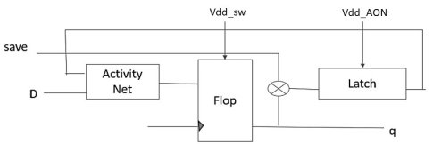
Figure 5
Figure 6 illustrates where isolation cells are introduced when a shutdown or a sleep phase is isolated from the receiving end. Isolation cells keep them turned off and block output to a predefined value. In these ways isolation cells are attached to reduce crowbar currents, thereby reducing power leakage.
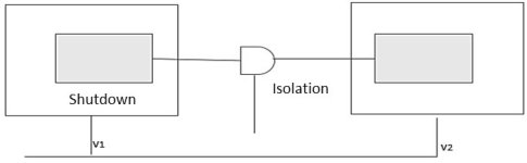
Figure 6
Clock Gating
This method is referred to as turning off the clock transitions when the circuit does not encounter switching of internal signals when there is no activity to be performed. This help controls the frequency of transitions from the power equation. Almost all EDA tools identify and support this.
The complexity of SoCs has expanded, introducing new demands for power management. The supply of the various SoC power domains must be flexible enough to be controlled by developers to control power dissipation and improve battery autonomy. Careful power analysis and knowledge of the capabilities of the tools at hand are prerequisites for selecting the best solutions. Power-related crises can be prevented by analysing power demand as early as possible in the design flow. Power goals are also made simpler to achieve by early analysis because higher-level techniques save the most power.


Comments
Post a Comment