Congestion in VLSI (Very large-scale Integration) design refers to the circumstance when the number of routing tracks is less than the required routing tracks. These routing resources are used to connect all the required wires between the different components of the design. PnR tool highlights congested areas as red hotspots, as depicted in figure 1. As the complexity of the design increases, congestion has become a major issue in chip design that requires careful consideration and optimization to ensure that the design meets the required timing, power, and area constraints.
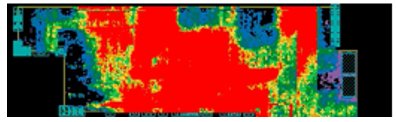
Fig-1
Congestion report:
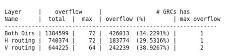
- GRC: The term GRC is an abbreviation of Global Routing Cells. During the initial placement, the core area gets divided into equally sized small squares called GRC.
- Overflow total: The summation of the total number of overflow routes for all GRCs. In the above report, it is 1,384,599.Overflow Max: “Both Dirs” means combined results for both horizontal and vertical routing directions. Max indicates the maximum number of overflow routes for a single GRC among all GRCs. For example, if there are 100 routing tracks available at a GRC while 172 tracks are going through it, that means the overflow is 72 for this GRC. Overflow (%): The GRCs value is the total number of global routing cells with any overflow/lack of routing resources. A GRC value of 426,013 indicates that 426,013 GRCs has an overflow among all GRCs. The overflow percentage (%) shows that out of the total number of GRCs, a certain percentage GRCs have overflow.
- Note: It has been observed that GRC overflow percentage should be less than 1%; otherwise, it would be difficult to route. If we proceed with routing with GRCs overflow (%) of 34.2291 as shown in the report, the PnR tool will still complete routing, but there will be lots of violations such as complex shorts and DRC violations. Additionally, the mentioned issues will cause timing degradation because it leads to an increase in the length of the interconnect wires, which increases the capacitance and resistance of the wires, thereby slowing down the propagation of the signal.
Cause of congestion:
- Bad floorplan/inappropriate placement of macros.
- High standard cell density in a particular area.
- High number of standard cells in close vicinity of macros, as shown in Figure 4.
- Routing blockages over standard cells, as shown in Figure 2.
- High port density, as shown in Figure 3.
- Scan chain reordering and mixing/swapping are restricted.
- Improper optimization of netlist during synthesis.
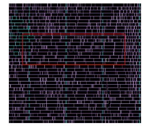
Fig-2
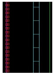
Fig-3
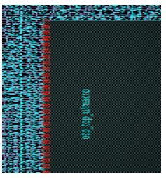
Fig-4
Congestion alleviation Techniques:
- Placement blockages
- Cell padding
- Keep out margin/HALO.
- Modify PG grid.
- Congestion driven placement.
- Try different techniques during synthesis like logical synthesis, topographical synthesis.
- SPG and non-SPG placement.
- Refine placement/floorplan.
- Placement blockages: Spread the standard cells if they are highly dense by creating partial placement blockages, as shown in Figure 5. Alternatively, restrict the placement of standard cells in a particular area if there is an immense lack of routing resources by creating hard placement blockages, as shown in Figure 6.create_placement_blockage -type partial -blocked_percentage 50 -boundary {{llx lly} {urx ury}} -name Partial_PB
- create_placement_blockage -type hard -boundary { {lrx lry} {urx ury} } –name Hard_PB
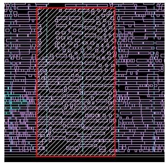
Fig-5
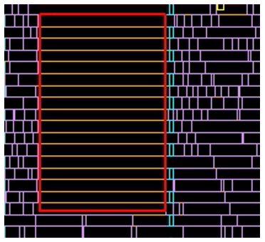
Fig-6
Keep out margin/Halo: Keepout margin is a region around the boundary of a macro in which no other cells are placed. Keeping the placement of cells out of such regions avoids congestion and net detouring and produces better Quality of result. In Figure –7, a keepout margin is created around the macro.
- create_keepout_margin -type hard -outer {5 5 5 5 } [get_cells *macro_name*]
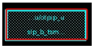
Fig-7
Cell padding: Applying a keepout margin around standard cells is known as cell padding. When a cell has a high number of pins like a multibit flop, the demand for routing resources increases. Hence, we restrict the placement of cells near these cells to avoid congestion.
Implementing cell padding:
- create_keepout_margin -type hard -outer {3.9200 3.9200 3.9200 3.9200} [get_cells cell_name]
- Refine_opt/incremental placement.
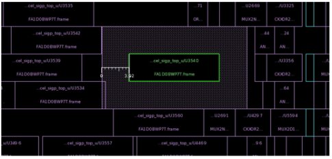
Fig-8
Modify PG grid: To have maximum routing resources, one can try to reduce the number of PG stripes or the width of stripes. However, this has a trade-off with electromagnetic (EM) and IR drop.
Topographic synthesis: At the very first stage, we perform logical synthesis and proceed to further stages like DFT, PnR. The synthesis tool tries to optimize in the best possible way to have a minimum netlist area and meet the required timing and power constraints. After one iteration of PnR we have floorplan information like block shape, size, blockages, and physical cells. We write out the DEF of the floorplan and give it back to the synthesis tool and rerun synthesis. Now it has physical constraints as well, so it will generate a more precise netlist. Eventually, this will have a low scope of congestion and other issues.
SPG and non-SPG placement: During topographical synthesis, the tool writes out DEF, which is equivalent to coarse/initial placement. Reading this DEF during placement for coarse placement is called SPG placement. If we don’t consider DEF for coarse placement and let the PnR tool, do it itself, it is non-SPG placement. One should try both techniques, as either one will be helpful for congestion alleviation.
- set_app_options -name place_opt.flow.do_spg -value true
- read_def -add_def_only_objects {cells} -convert_sites <def file>
- Place_opt
Congestion related variable:
- set_app_options -name place_opt.place.congestion_effort -value high
- set_app_options -name place.coarse.cong_restruct_effort -value ultra
- set_app_options -name place.coarse.congestion_layer_aware -value true
- Refine placement: The refine placement performs incremental congestion optimization for congested designs. One should perform this after detailed placement.refine_placement -effort high -congestion_effort high
Shorts: When the shape (small segment of net) of two different nets intersects/touches each other in the same layer, a short is reported. As depicted in Figure –9, the small portion of the red highlighted net is touching the yellow highlighted net. Since both nets are different and in the same metal layer, a short occurs.
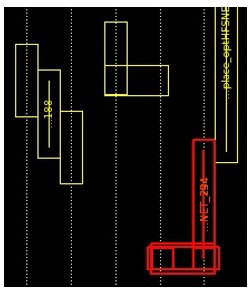
Fig-9
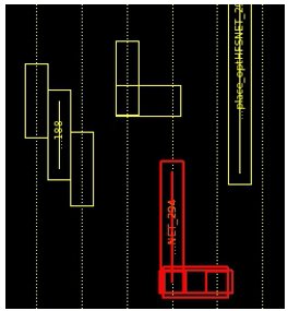
Fig-10
Mitigation: As depicted in Figure10, shift the the red highlighted net to the left. Now, they don’t interfere with each other, and the short is fixed. To verify and report shorted nets, run one of the following commands:
- Check_routes
- Check_lvs
If the design has shorts in single or double digits, they can be fixed manually quickly and easily. However, if the design has shorts in multiple thousands, the following approaches are preferred to get rid of shorts.
1. Delete shorted nets and reroute them by running eco route while freezing the rest of the nets.
To remove shorted nets:
- Remove_routes -detail_route -global_route -shield_route -nets “$net_nam”
To route the removed nets:
- route_eco -open_net_driven true.
2. Run “route_detail”, which performs detail routing to help fix shorts and DRCs. The following command performs detail routing with a maximum iteration of 5. Try running multiple loops of route_detail with increasing values of max_number_iterations to minimize DRCs and shorts.
- route_detail –max_number_iterations 5
3. If there are shorts at corners of the design, especially in a rectilinear shape, to fix such shorts, add a decent-sized routing blockage, as shown in Figure 11, at the shorted corner of the design during the floorplan stage. Remove it during the routing stage once the detail route is done. After removing the blockages, perform incremental detail route as demonstrated below.
- remove_routing_blockages *corner_blockages*
- route_detail -incremental true
Fig-11
4. If there are shorts in a specific layer’s region, to fix such shorts, limit the number of routings in that layer by applying a routing guide. A Routing guide must be applied during the placement stage only. In the example below, we are only considering 70 % of the routing resources of metal layer M2 to limit the routing.
Set bbox {{ 1125.8800 -210.1300} { 1404.2000 747.9400}}
create_routing_guide -layers METAL2 -vertical_track_utilization 70 -boundary $bbox -name rg1.
refernce:ishu sukla

Comments
Post a Comment