In a VLSI design, floorplan is the crucial stage in which chip area, size and shape of the chip can be determined. Floorplan is iterative process. When designer is done with the floorplan, the next step is to run placement and optimization, after completion of placement and optimization designer would analyse the congestion map, cell density and timing reports, before moving to next stage i.e. Clock Tree Synthesis. This article discusses about the various approaches to reduce congestion and timing violation by modifying floorplan at block level.
- Minimize the total wire length.
- Improve routability.
- Minimize delay.
- Minimize cost
At placement and optimization stage, PnR Tool tries to optimize data path so that data arrival time can be minimized and worst negative slack (WNS) and total negative slack (TNS) could be reduced. Placement is the process of finding a suitable physical location for each cell in the design. The quality of routing in design is highly determined by the placement. If more number of cells are placed in a small area then the number of routing tracks available for routing is less than the required routing tracks, which may cause congestion in the design. There are several reasons for congestions:
- High standard cell density in a small area.
- Placement of standard cell near macros.
- High pin density at the edge of the macro.
- Bad floorplan.
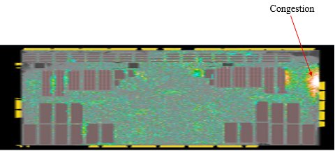
Figure 1. Congestion near the port
Congestions near the port is shown in figure 1. The designer must take care of these issues at the beginning by applying placement blockages (soft, hard, partial blockage), keep-out margin, Scan chain Re-ordering, cell padding, macro padding and create bounds. Creating bound allows the user to define region-based placement.
causes of congetion:
- Bad floorplan/inappropriate placement of macros.
- High standard cell density in a particular area.
- High number of standard cells in close vicinity of macros.
- Routing blockages over standard cells
- High port density
- Scan chain reordering and mixing/swapping are restricted.
- Improper optimization of netlist during synthesis.
Congestion alleviation Techniques:
- Placement blockages
- Cell padding
- Keep out margin/HALO.
- Modify PG grid.
- Congestion driven placement.
- Try different techniques during synthesis like logical synthesis, topographical synthesis.
- SPG and non-SPG placement.
- Refine placement/floorplan.
- Placement blockages: Spread the standard cells if they are highly dense by creating partial placement blockages, as shown in Figure 5. Alternatively, restrict the placement of standard cells in a particular area if there is an immense lack of routing resources by creating hard placement blockages, as shown in Figure 6.create_placement_blockage -type partial -blocked_percentage 50 -boundary {{llx lly} {urx ury}} -name Partial_PB
- create_placement_blockage -type hard -boundary { {lrx lry} {urx ury} } –name Hard_PB
Keep out margin/Halo: Keepout margin is a region around the boundary of a macro in which no other cells are placed. Keeping the placement of cells out of such regions avoids congestion and net detouring and produces better Quality of result. In Figure –7, a keepout margin is created around the macro.
- create_keepout_margin -type hard -outer {5 5 5 5 } [get_cells *macro_name*]
Cell padding: Applying a keepout margin around standard cells is known as cell padding. When a cell has a high number of pins like a multibit flop, the demand for routing resources increases. Hence, we restrict the placement of cells near these cells to avoid congestion.
Implementing cell padding:
- create_keepout_margin -type hard -outer {3.9200 3.9200 3.9200 3.9200} [get_cells cell name]
- Refine_opt/incremental placement.
Cell padding: Applying a keepout margin around standard cells is known as cell padding. When a cell has a high number of pins like a multibit flop, the demand for routing resources increases. Hence, we restrict the placement of cells near these cells to avoid congestion.
Implementing cell padding:
- create_keepout_margin -type hard -outer {3.9200 3.9200 3.9200 3.9200} [get_cells cell_name]
- Refine_opt/incremental placement.
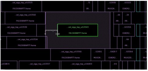
Fig-8
Modify PG grid: To have maximum routing resources, one can try to reduce the number of PG stripes or the width of stripes. However, this has a trade-off with electromagnetic (EM) and IR drop.
Topographic synthesis: At the very first stage, we perform logical synthesis and proceed to further stages like DFT, PnR. The synthesis tool tries to optimize in the best possible way to have a minimum netlist area and meet the required timing and power constraints. After one iteration of PnR we have floorplan information like block shape, size, blockages, and physical cells. We write out the DEF of the floorplan and give it back to the synthesis tool and rerun synthesis. Now it has physical constraints as well, so it will generate a more precise netlist. Eventually, this will have a low scope of congestion and other issues.
SPG and non-SPG placement: During topographical synthesis, the tool writes out DEF, which is equivalent to coarse/initial placement. Reading this DEF during placement for coarse placement is called SPG placement. If we don’t consider DEF for coarse placement and let the PnR tool, do it itself, it is non-SPG placement. One should try both techniques, as either one will be helpful for congestion alleviation.
- set_app_options -name place_opt.flow.do_spg -value true
- read_def -add_def_only_objects {cells} -convert_sites <def file>
- Place_opt
Congestion related variable:
- set_app_options -name place_opt.place.congestion_effort -value high
- set_app_options -name place.coarse.cong_restruct_effort -value ultra
- set_app_options -name place.coarse.congestion_layer_aware -value true
- Refine placement: The refine placement performs incremental congestion optimization for congested designs. One should perform this after detailed placement.refine_placement -effort high -congestion_effort high
Shorts: When the shape (small segment of net) of two different nets intersects/touches each other in the same layer, a short is reported. As depicted in Figure –9, the small portion of the red highlighted net is touching the yellow highlighted net. Since both nets are different and in the same metal layer, a short occurs.
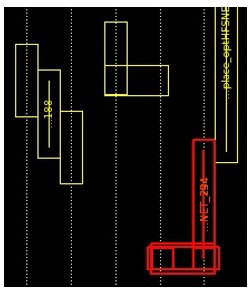
Fig-9
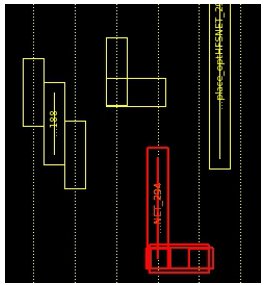
Fig-10
Mitigation: As depicted in Figure10, shift the the red highlighted net to the left. Now, they don’t interfere with each other, and the short is fixed. To verify and report shorted nets, run one of the following commands:
- Check_routes
- Check_lvs
If the design has shorts in single or double digits, they can be fixed manually quickly and easily. However, if the design has shorts in multiple thousands, the following approaches are preferred to get rid of shorts.
1. Delete shorted nets and reroute them by running eco route while freezing the rest of the nets.
To remove shorted nets:
- Remove_routes -detail_route -global_route -shield_route -nets “$net_nam”
To route the removed nets:
- route_eco -open_net_driven true.
2. Run “route_detail”, which performs detail routing to help fix shorts and DRCs. The following command performs detail routing with a maximum iteration of 5. Try running multiple loops of route_detail with increasing values of max_number_iterations to minimize DRCs and shorts.
- route_detail –max_number_iterations 5
3. If there are shorts at corners of the design, especially in a rectilinear shape, to fix such shorts, add a decent-sized routing blockage, as shown in Figure 11, at the shorted corner of the design during the floorplan stage. Remove it during the routing stage once the detail route is done. After removing the blockages, perform incremental detail route as demonstrated below.
- remove_routing_blockages *corner_blockages*
- route_detail -incremental true
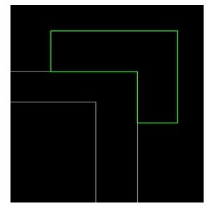
Fig-11
4. If there are shorts in a specific layer’s region, to fix such shorts, limit the number of routings in that layer by applying a routing guide. A Routing guide must be applied during the placement stage only. In the example below, we are only considering 70 % of the routing resources of metal layer M2 to limit the routing.
Set bbox {{ 1125.8800 -210.1300} { 1404.2000 747.9400}}
create_routing_guide -layers METAL2 -vertical_track_utilization 70 -boundary $bbox -name rg1
2. Design Challenges
In this two challenges would be discussed: -
- Congestion near to the feedthrough port, most of the cells placed near the port and forms the crisscross path with another port.
- Another challenge is to Reg2out violation. In this case, 48 flip flop are placed at one location and interacting with all macros placed at left side and the port placed at left top of the design.
Case 1: fixing congestion near feedthrough port
This section describes a port swapping technique by which congestion can be reduced near the ports. While doing swapping of the port, designer has to take care of the other block also. If that port of the block is interacting with other blocks, then swapping of the ports will be done accordingly. In the figure 2, top ports that are pink in color represent feed_input ports and feed_output port on the right bottom side. Similarly, for blue color top right side is feed_output and right one is feed_input port. Instances that are highlighted in blue and pink color are registers.
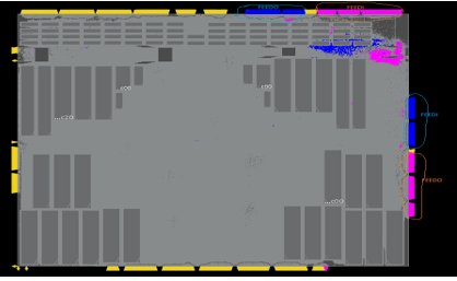
Figure 2.feed_input and feed_output ports
In figure 3, Top right feed_input ports which are in blue color are interacting with feed_output port which is green in color which is placed on right edge of the block and we see there is one pipe line registers between them which is shown by yellow color line.
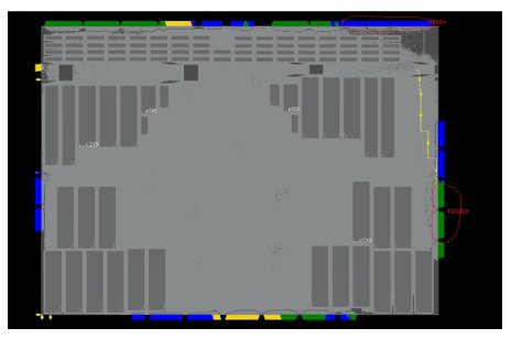
Figure 3. Interaction between feed_input and feed_output ports
Implementation:
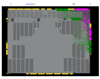
Figure 4 After swapping feed_input and feed_output ports
As shown in figure 4, right side feed_input* ports are swapped with feed_output* ports to improve congestion by reducing criss-cross near the ports. After implementing this Congestion improved from 4.4% to 2.2%.
Case 2: Fixing Register to output (REG2OUT) setup violation-
At floorplan stage, Macro/IP placement, pin/port placement and power planning are performed. Only setup violations would be reported at placement stage, and hold violations will be reported after CTS stage in Pnr flow.
Path groups would be creating for the timing path. This enables reporting the timing results separately for each group, as well as set the options to focus the timing optimization on specific critical timing path groups.
Command (in Innovus) createBasicPathGroups – expanded can be used to create reg2reg, reg2Cgate, in2reg, reg2out, and in2out path groups.
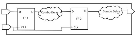
Figure 5 : Different timing path groups
In the above figure path between flip-flop 1 and flip-flop 2 is called as reg2reg path and the path between flip-flop 2 and the output port is called as reg2out path. The reg2reg and reg2cgate default path groups are high effort path groups for optimization and the remaining path groups are low effort path groups. We can also create custom path groups according to the requirement. STA person would define constraints for I/O timing e.g. input delay, external delay etc. in Synopsys design constraint (SDC) file. Virtual clocks are defined to constraint the I/O timing paths. While doing PnR at block-level, I/O timing should be met even though internal timing has the higher priority. While doing timing optimization, tool will locate flip-flops according to timing requirements. As internal timing has higher priority, it might be possible that the tool would place flip-flops little away from the I/O port.
METHODOLOGY: -
To fix IO timing violation, we need to analyze the cause of the timing violations so that it can be fixed at the right stage. In this design, reg2out setup violation reported at placement stage. To meet the internal timing, tool placed those flops a little away from the output port. These violations need to be addressed at the placement stage itself. It was found that there was enough margin in previous timing paths (reg2reg). So flopbound could be created near the output port to fix the reg2out setup violations. Now there are few things that need to be identify: -
- location of the bound
- Size of the bound
- Which group should be created out of soft Guide, Guide, Region and Fence.
PnR tool, Innovus support four type of physical floorplan constraints namely soft guide, guide, region and fence.
Soft Guide: -
Soft guide constraints are similar to a guide constraint except that there are no fixed locations. The soft guide constraints are not as restrictive as a fence or region constraint, so some instances/cell might be placed further away if there are talking to other modules.
Guide:
It roughly defines an area within which the PnR tool place instances/cells of given module. Instances from modules that are not part of the guide might be placed inside the guide if the area of the guide is underutilized. Similarly, cells from the modules defined as the part of the guide may be placed outside if the area of the guide is over utilized. So basically, a guide is a soft indicant for the placement of the cell that may let some cells in and let some cells out.
Region:
The region constraint is also a loose constraint. However, it is stronger than the guide constraint. When region is created, it requires all the cells of the modules contained in the defined region to be placed in the specific region area. If there is an extra space in the region, other cells from the other modules might be placed inside.
Fence:
The fence constraint is the strongest floorplan constraint. It would not allow cells from other modules to be placed inside even if the area is underutilized. Additionally, the cells in a fenced area cannot be placed outside the defined fence area.
Now it is very important to choose which type of physical floorplan constraints need to be selected for creating the flop bound. Four types of floorplan constraints have been described above.
For this case, a region had been created as the flops would be placed together and at the specified location, moreover, other cells from other modules could also be placed inside region if some extra space would be there, hence the area can be utilized completely. The distance between the output port and the bound depends on the setup slack of violating timing paths and the margin available in the previous paths. Finding the appropriate location of the flip-flop bound is an iterative process.
First, the designer has to select one location based on parameter described earlier and checked the timing violations, if violation had not been reduced to the desired limit, then the flop bound would be shifted nearer to output port and then again check the timing report. If the slack of timing path is under the desired limit, that would be the final location of the flop bound. Cells those need to be pulled inside the bound would be selected before creating the region for the flops. Start by creating an instance group and assigning members to the group. Then region would be created using the group name.
Implementation:
In the design, a region of 48 flops has been created near the output port and it would prevent the spreading of those flops. Hence, reg2out setup violations can be reduced to the desired limit.
Specification of block
Dimension | 2126 x 976.68 |
Instances | 1.06 M |
Utilization | 17% |
Macro count | 220 |
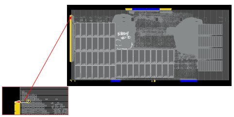
Figure6: Interaction of 48flops with highlighted macros at first level
In the figure shown above, output port has been highlighted and placement of the registers has been shown before creating region.
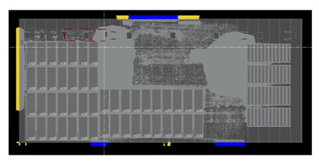
Figure7. bound of 48 flops
In this figure, location of the region has been shown in the design. It makes sure that internal timing should not get violated while fixing reg2out timing violations. Reg2out setup timing violation reduced to desired limit after implementation of above methodology.
CONCLUSION:
Floorplanning is an important and critical step of the PnR flow. If the quality of floorplan is not remarkable, it can create different issues like congestion, timing violations, routing issues and IR drop etc. Few real design scenarios have been discussed here. Placement of feedthrough ports at the appropriate location is required to control the congestion and reduce the cell density at the specified area. For I/O timing violations, identifying real cause is essential to apply the required approach for fixing the violations.
Creating bound could be one approach to address the I/O timing violations at floorplan stage. This would also help in reducing the number of buffers/inverters inserted by the tool for the optimization in I/O timing paths. Size and location of the bound should be selected carefully by the designer. Multiple bounds can be created in the design as per the requirement.

Comments
Post a Comment